Intermediate Band Solar Cell
Graphical user interface
Here we concentrated the information about the use of a simulator intent to help with the understanding of Intermediate band solar cells.
Click the link below to download the executable for Windows operational system.
IBSC – SimulationWindows Operational System |
IBSC – SimulationLinux Operational System |
Basic information about solar cells
Solar cells are optoelectronic devices able to generate an electric current from the absorption of light irradiated by the sun. They are formed by sandwiching doped (n- and p-type) and undoped (i-type, intrinsic) semiconductor layers, forming a p-i-n junction.
The semiconductors forming the solar cell are classified by their energy bands. Namely, the valence band VB (formed by fully occupied electronic states – at absolute zero temperature) and the conduction band CB (formed by fully unoccupied electronic states – at absolute zero temperature). VB and CB are split apart by a bandgap where no electronic states exist. The more energetic electrons in the top of VB can absorb photons shed on the device e be excited across the bandgap up to the CB, populating the empty states. The mobility of electrons in CB is high, allowing for electronic movement, in other words – electronic current.
When the light is shed on the solar cell, electrons are promoted to the beforehand empty state. However, to generate a net current is mandatory an electric field to accelerate the carriers. Such an electric field is determined by the doped layers forming the p-i-n junction. The potential difference among the layers bends the intrinsic region of the solar cell, forming an intrinsic electric field able to drain photo-generated electrons as a net current. See figure 1. The states left empty after excitation also contributes to the current, forming quasi-particles called holes.
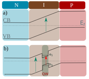 |
| Fig 1: Formation of a p-i-n junction. (a) Top of valence band and bottom of conduction band separated by the bandgap, forming the potential profile of a basic p-i-n junction. Electrons can be excited crossing the bandgap and extract toward the doped layer by the intrinsic electric field of the cell, generating a net current. (b) The same p-i-n junction added to a lower bandgap additional layer within the intrinsic one, forming a quantum well potential profile. The excitation occurs across both the host semiconductor (green arrow) and inside the quantum well (red arrow). |
The separation between BV and BC determines the minimum energy necessary to shed photons excite electrons. This way, the solar cell absorption is limited by the material’s bandgap, also limiting its efficiency. Solar cells are transparent to photons lesser energetic than the host semiconductor bandgap.
To raise the efficiency, additional absorption channels are required allowing for lesser energetic photons to be collected end converted into current. One option is to place within the intrinsic layer a different semiconductor with a smaller bandgap than the host semiconductor, with a width of the order of the electron’s de Broglie wavelength. The inclusion generates a quantum-well-like potential profile, with bound states both in BV and BV. See figure 1(b). The transition between the bound states generates a new pathway to excite electrons with less energetic photons, increasing the overall light-to-current conversion efficiency.
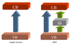 |
| Fig 2: Schematics of the excitation process in a single junction cell (left panel) and in an intermediate band cell (right panel). |
Figure 2 shows schematics of the excitation processes in a single junction solar cell (left panel) and in a cell with an additional band between VB and CB. As we can see, the only way of exciting electrons from VB to CB in a single junction is by the absorption of photons with energies greater than the separation of the bands. A whole spectrum of photons is missed. To overcome such a limitation, an additional band can be put inside the bandgap, the so-called intermediate band (see the right panel of figure 2). Such a band can be achieved by using impurities. but also can be related to quantum, well’s bound states. The device equipped with intermediate states is called the Intermediate band solar cell. The addition of extra absorption paths increases the cell’s efficiency.
Simulator Overview
This is a Python implementation of a GUI wrapper for the Fourier Grid Hamiltonian method employed in the analysis of Quantum Well-based Intermediated band solar cell.
 |
|---|
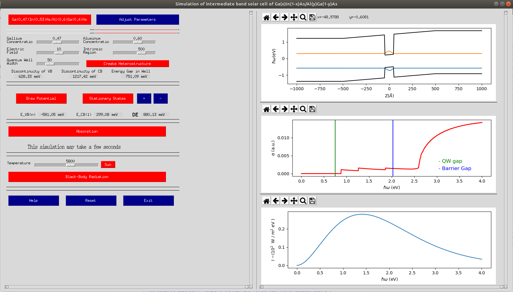
| Fig. 3: General view of the GUI |
Figure 1 shows the main interface. The IBSC is simulated from a p-i-n semiconductor junction, where a semiconductor with a lesser bandgap (forming the QW layer) is sandwiched between two layers of a bigger gap semiconductor (forming the barriers). At the present moment, the barriers are formed by , and the QW is formed by
.
The Quantum Well is in the intrinsic (non-dopped) region of the p-i-n junction. The n- and p-type dopping generates an intrinsic electric field that bends the i-layer. When light is shed on the structure, electrons from the valence band (VB) are excited towards the conduction band (CB), unbalancing the charge in the structure. Connecting the contacts, a short-circuit current is created with both the electrons being drifted at CB and the holes drifted at VB.
To control the current generation, several structural parameters can be set:
* Quantum Well Width
* Quantum Well height
* Intrinsec electric field
* p-i-n intrisic layer width
The GUI allows for controlling such parameters or using standard ones by just clicking the buttons, as shown in fig. 4.
 |
|---|
| Fig. 4: Choosing parameters |
The concentration of each element defines the energy bandgap. The misalignment between the different layers put together determines the potential profile of the structure. In the simulation, the concentration of the elements for the barrier layer and the quantum well layer can be adjusted. Therefore, the band offset (related to the difference between the layer’s gap distributed across valence and conduction bands) can be adjusted determining the quantum-well heights.
The interface also allows for adjusting the quantum well width, as well as the size of the intrinsic region of the p-i-n junction, and the built-in electric field. After choosing the parameters, the potential profile could be plotted. The interface will display the band offsets and the quantum well bandgap at the right-hand-side panel.
After choosing the structure’s parameters, the potential profile can be visualized by plotting it.
 |
| Fig 5: Detail of the plotting commands. |
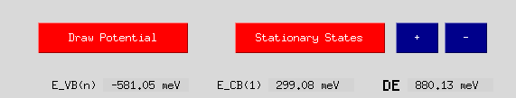
Once the potential is defined, the eigenstates and eigenfunction can be calculated. This is accomplished by solving Schroedinger’s equation. In the simulation, just hit the button “Evaluate States”. The “+” and “-” buttons add and remove states from the plot easing the visualization.
The next step to evaluate the working of the solar cell is to calculate the absorption. It is done using the pre-calculated states. By pressing the button “absorption” the calculation is performed and a graph with the results is shown. The vertical bars in the graph will determine the semiconductors’ bandgaps, allowing for direct visualization of the consequence of adding the quantum well to the structure.
Finally, the simulator also evaluates the solar spectrum emission as the black body emotion. By comparing the absorption with the solar emission spectrum, we can see how the introduction of the intermediate state can favor the absorption of more photons in comparison to the response of the single-junction solar cell.
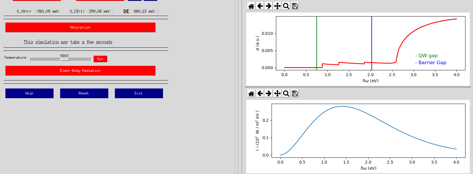 |
| Fig 6: Detail showing the absorption and the solar emission spectrum. |